
The Machine Behind the Machine: ASML and America’s AI-Quantum Industrial Future
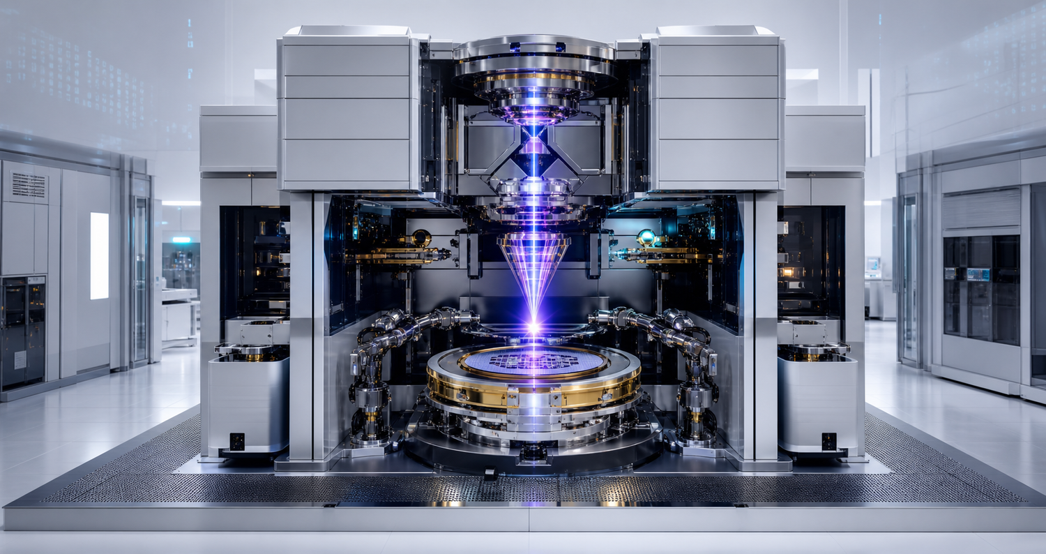
ASML is the machine behind the machine. The public story of artificial intelligence is usually told through model releases, data centers, GPUs and power demand. The public story of quantum is usually told through qubit counts, error correction and national research programs. Beneath both sits a more physical bottleneck: the ability to pattern matter at industrial scale with enough precision, throughput and repeatability to make advanced chips real. That bottleneck has a name, a geography and a supply chain. The name is ASML. The geography begins in Veldhoven and fans out through Zeiss optics, Cymer light sources, American, European and Asian component suppliers, and the fabs of Taiwan, Korea, the United States, Japan and Europe. The supply chain is large enough to be global and narrow enough to be strategic.
The July intelligence read is simple: America’s semiconductor future will be decided partly by fabs, subsidies and chip design, but also by how well the United States understands lithography as an operating constraint. ASML’s current public record is larger than the 2024 baseline: the company reported 2025 net sales of €32.7 billion, research and development of €4.7 billion, 535 system sales, a supplier base of about 5,100 companies, and Q1 2026 net sales of €8.8 billion. Those figures describe a scarce industrial organism. A country can appropriate money for fabs in a single legislative season. It cannot instantly reproduce a supplier web that took decades, more than €6 billion of EUV R&D investment over 17 years, and repeated customer co-development to mature.
Practical takeaway. For America, ASML is neither a foreign vendor footnote nor a diplomatic inconvenience. It is a timetable for AI capacity, a gating layer for advanced memory and logic, and a test of whether allied industrial strategy can manage chokepoints without freezing innovation.
The tool that sets the cadence of AI
EUV lithography matters because it changes what a fab can print economically. ASML’s EUV systems use 13.5 nanometer light, almost in the X-ray range, to pattern the most intricate layers of advanced microchips. ASML states that it is currently the world’s only manufacturer of EUV lithography systems. Its NXE platform, introduced to customers in 2013 and now widely used in high-volume manufacturing, supports the advanced logic and memory roadmaps that sit behind AI accelerators and high-bandwidth memory. The newer NXE:3800E increases productivity by more than 35 percent compared with the NXE:3600D, according to ASML’s 2024 annual report. That percentage is more than an engineering upgrade. It changes queueing, cycle time, depreciation economics and the number of wafers that can pass through the tightest part of the factory.
High-NA EUV moves the argument one stage deeper. ASML’s EXE systems use a 0.55 numerical aperture and, according to the company’s EUV systems page, are designed to print with a resolution of about 8 nanometers while supporting high-volume manufacturing in the 2025–2026 period. ASML says the platform will enable geometric scaling into the next decade, starting at the 2 nanometer logic node and followed by memory nodes at similar density. In 2024, ASML finalized the first installation of its TWINSCAN EXE:5000 High-NA EUV system at a major customer. That event is a small sentence in an annual report and a large fact in the industrial calendar. AI demand is hungry for leading-edge logic, dense memory and energy efficiency. High-NA is one of the tools that decides how far that appetite can be met with manufacturable silicon instead of slideware roadmaps.
The ASML constraint also corrects a common American habit. Washington often speaks about chips as if the strategic unit were the fab. In practice, the fab is a choreography of tools, recipes, chemicals, masks, software, optics, maintenance contracts, field engineers and yield learning. ASML does not replace foundry skill, EDA, packaging, materials or design. It sets a hard physical tempo for the most valuable layers. If EUV tool deliveries slip, if service capacity is thin, if spare parts are constrained, or if export-license uncertainty changes the backlog, downstream AI plans feel it as delay, cost and uncertainty. The bottleneck is not theatrical. It appears as missed wafer starts, lower utilization, longer qualification and slower node migration.
Quantum hardware also lives in the lithography stack
Quantum computing is more heterogeneous than AI silicon. Superconducting circuits, spin qubits, trapped ions, neutral atoms, photonics and topological approaches do not share a single manufacturing path. Many laboratory devices still rely on small-batch fabrication, electron-beam lithography, bespoke materials, university cleanrooms and research foundries. That makes it tempting to treat ASML as a semiconductor-only story. The temptation is too narrow. Scalable quantum systems will need better patterned devices, lower variation, denser interconnects, cryogenic control electronics, photonic interfaces, classical co-processors and packaging that can survive temperature, noise and reliability requirements. Those are manufacturing questions before they are branding questions.
The quantum implication is indirect and powerful. EUV will not be the right tool for every qubit layer. It may be excessive for some experimental devices and unsuitable for others. Yet the industrialization of quantum hardware will borrow the habits of advanced semiconductor manufacturing: process control, overlay accuracy, defect inspection, metrology, wafer-level repeatability, design rules and supply-chain discipline. ASML’s world is the world in which fragile devices become repeatable products. The same national capacity that gives America reliable access to leading-edge logic also supports the control chips, cryo-CMOS research, silicon photonics and advanced packaging ecosystem around quantum machines.
There is a further American consequence. If quantum remains a laboratory race, the United States can win through universities, national labs, defense programs and venture capital. If quantum becomes a manufacturing race, it will test the same tool access, supplier resilience and process-engineering depth that already shape AI silicon. Lithography is therefore a bridge between two policy communities that too often work in parallel: AI compute planners and quantum technology strategists. Both need the same uncomfortable answer. Breakthrough science must eventually pass through a factory, and the factory has chokepoints.
Export controls turned lithography into alliance law
ASML’s tools now sit inside a legal architecture as much as a factory architecture. The United States, the Netherlands and Japan have progressively tightened controls on advanced semiconductor manufacturing equipment and related advanced computing items. The U.S. Bureau of Industry and Security’s October 2023 rules separated two linked tracks: semiconductor manufacturing equipment controls and advanced computing / supercomputing controls. In December 2024, BIS added foreign-produced direct product refinements, new controls for semiconductor manufacturing equipment and related items, high-bandwidth memory controls, and entity-list changes. The legal language is technical. The strategic object is plain: slow the ability of destinations and entities of concern to produce advanced-node integrated circuits and high-end AI compute.
The Dutch role is decisive because ASML is Dutch. ASML’s annual report describes export controls, sanctions compliance and technological sovereignty as material operating issues. It also notes that export controls affected customer caution and demand planning, while the company continued delivering non-advanced lithography systems not impacted by new restrictions. China demand in 2024 was supported by backlog built in previous years, with ASML expecting a shift toward more normalized China sales levels after that backlog was fulfilled. That is how geopolitics enters the income statement: not through speeches, but through licenses, backlog timing, product segmentation and customer capital expenditure.
Export controls create a paradox for America. The United States benefits from limiting rival access to advanced tools and AI chips, yet it also depends on allied companies whose commercial incentives, domestic politics and customer relationships are not identical to Washington’s. A control that is too porous fails strategically. A control that is too abrupt can push demand toward substitution, stockpiling, diplomatic resentment or gray-market engineering. A control that is narrow on paper but broad in service implications may create hidden operational effects. The intelligent position is not maximalism. It is calibration: define the controlled capability, coordinate with allies before surprise, monitor actual manufacturing capability instead of headlines, and preserve incentives for ASML, its suppliers and its customers to keep investing in the open allied ecosystem.
The supply-chain chokepoint is wider than Veldhoven
ASML is scarce partly because its suppliers are scarce. The 2025 annual report lists about 5,100 suppliers: 1,600 in the Netherlands, 700 in the rest of EMEA, 1,350 in North America and 1,450 in Asia. That geographic spread matters. The company is Dutch, but the machine is transnational. The United States is not outside the lithography stack. American suppliers, Cymer light-source heritage, software, precision components and customer fabs are inside it. This is why a crude autonomy slogan misses the point. The relevant question for America is not whether it can nationalize every layer of the stack. It is whether it can make the allied stack more reliable, more serviceable and harder to coerce.
The chokepoint has several layers. First is tool manufacturing capacity: how many EUV and High-NA systems can be built, qualified and shipped. Second is installation and service: a scanner is not a boxed commodity; it is a living system that requires field engineers, cleanroom integration and continuous performance management. Third is upstream specialization: optics, lasers, stages, sensors, mechatronics, vacuum systems and ultra-clean components. Fourth is customer concentration: ASML itself warns that lithography systems are sold to a limited number of customers, and consolidation can increase dependency. Fifth is policy friction: export licenses, sanctions, end-use rules, foreign direct product rules and allied politics. A modern AI strategy that treats any one of these as secondary is leaving risk unpriced.
America’s CHIPS policy should be read through this operational lens. NIST’s CHIPS for America program frames semiconductors as integral to economic and national security, powering consumer electronics, automobiles, data centers, critical infrastructure and military systems. The incentive program, the National Semiconductor Technology Center, packaging initiatives and metrology work are necessary pieces. Yet fab construction without tool-flow realism becomes a ribbon-cutting strategy. The United States needs to know where EUV capacity will be booked, how High-NA insertion will affect process choices, whether domestic fabs have enough trained lithography engineers, how quickly service teams can respond, and where a single supplier failure could halt a module. The policy word is resilience. The factory word is uptime.
Practical consequences for America
First, fab policy must include tool diplomacy. The United States can subsidize domestic capacity, but the most advanced scanners are allocated through commercial relationships, customer roadmaps and ASML’s own ramp. American policy should therefore treat ASML, the Dutch government, Japanese equipment firms, Taiwanese and Korean foundries, and U.S. tool suppliers as one strategic conversation. The goal is not to bully the toolmaker. The goal is to make American capacity credible enough to earn priority: reliable permitting, predictable power, trained labor, supply-chain readiness and customers whose volumes justify tool placement.
Second, export controls need service-level thinking. Controls often focus on shipment of named tools or chips. The operational world includes software updates, spare parts, field service, maintenance knowledge, performance upgrades and training. If a controlled ecosystem can be kept alive through service channels, the control underperforms. If legitimate allied fabs are caught in ambiguity, the control damages friendly capacity. The most valuable export-control office is therefore not only a licensing gate. It is an intelligence function that understands how a lithography tool lives after shipment.
Third, America needs more lithography people. The shortage is not simply electrical engineers in the abstract. It is process engineers, field technicians, optics specialists, mechatronics experts, contamination-control professionals, metrology scientists, computational lithography teams and managers who can run yield learning without drama. ASML’s 44,027 FTE figure gives scale to the human system behind the machines. A workforce plan that trains generic semiconductor enthusiasm but neglects lithography operations will produce speeches faster than wafers.
Fourth, quantum programs should connect earlier to semiconductor manufacturing discipline. National quantum strategies often fund devices, algorithms and networking. They should also fund process-control bridges: quantum-compatible materials, low-defect patterning, cryogenic interconnects, wafer-level testing, photonic integration, and packaging methods that can be transferred into industrial lines. The point is not to force every quantum architecture into a CMOS template. It is to prevent the common valley of death where a brilliant device cannot be manufactured repeatably enough to become infrastructure.
Fifth, AI infrastructure planning must count lithography as an energy policy variable. Advanced nodes improve performance per watt; AI data centers then create new power demand by scaling use. If lithography delays slow access to more efficient accelerators and memory, America may end up buying more energy, more cooling and more floor space to produce the same compute. The scanner in the cleanroom is therefore connected to the substation outside the data center. That connection is rarely visible in AI policy, but it is economically real.
The future strategic outlook: 2026 to 2030
The next phase will be less forgiving than the last one. High-NA EUV insertion, AI-driven demand, high-bandwidth memory pressure, export-control adaptation and quantum-device industrialization will collide in the same planning window. From 2026 onward, the leading question will be which customers can absorb High-NA cost and process change quickly enough to turn physics into yield. The winners will not simply be the buyers with access to the newest machine. They will be the organizations with masks, resists, metrology, process integration, computational lithography and design-technology co-optimization ready around the machine.
China will keep searching for substitutes. Export controls can slow access to the highest-end lithography and manufacturing equipment, but they also create incentives for domestic tool development, workarounds, mature-node expansion and strategic stockpiling. The allied objective should be measured realistically. Controls can preserve a moving frontier if the frontier keeps moving. They cannot become a substitute for investment. If America and its allies slow their own tool deployment, workforce development or next-node economics, a defensive control regime will become brittle.
Europe will matter more, not less. ASML gives the Netherlands a role in global technology politics that exceeds the size of the Dutch economy. Zeiss gives Germany a deep optical stake. Imec gives Belgium a research bridge into future nodes. Japan remains crucial in equipment and materials. Taiwan and Korea carry manufacturing depth. The United States remains essential in design, EDA, equipment components, cloud demand, defense use and now industrial policy funding. No single capital owns the stack. The mature American posture is alliance competence: fewer surprise demands, more shared roadmaps, faster permitting, better intelligence, and enough humility to know where allied capability is irreplaceable.
How Quentir Reads It
For Quentir, ASML is the kind of strategic object that rewards continuous reading. It links corporate reporting, export law, national security, AI infrastructure, quantum manufacturing and supply-chain risk in one machine. That is why this post sits naturally beside Quentir’s broader intelligence archive and why readers who need the running file should use the All-access membership: the value is not one headline about a scanner, but the accumulation of dated signals as tools, controls and customers move. The coming years will not ask whether lithography is important. They will ask who understood it early enough to plan around its constraints.
The strategic outlook is therefore sober and constructive. America can benefit enormously from ASML without owning it. It can build fabs that deserve the most advanced tools. It can coordinate export controls without poisoning allied incentives. It can connect quantum programs to manufacturing reality before the scaling problem becomes embarrassing. That is also the point of Mauritz Kop’s War on the Rocks argument for a Bletchley Park for the quantum age: quantum security is not produced by isolated laboratories alone, but by allied feedback loops among science, engineering, standards, export controls and operational verification. In the ASML context, that Bletchley-style discipline becomes physical: without trusted access to advanced patterning, metrology, optics, service capacity and the supplier base around them, AI-quantum strategy remains a concept instead of deployable capacity. It can treat AI compute as a full stack of power, chips, memory, lithography, packaging and law. The quiet fulcrum is visible now. The countries and companies that organize around it will move faster than those that discover, too late, that their semiconductor strategy stopped at the fab wall.
Published intelligence, built to inform your own decisions. Published: July 7, 2026.
Sources checked July 7, 2026: ASML 2025 Annual Report and 2025 US GAAP PDF; ASML Q1 2026 financial results; ASML 2024 Annual Report and 2024 US GAAP PDF for first High-NA installation and 2024 product details; ASML EUV lithography systems; ASML DUV lithography systems; Federal Register / BIS rules: Export Controls on Semiconductor Manufacturing Items (Oct. 25, 2023), advanced computing and supercomputer controls (Oct. 25, 2023), April 2024 corrections and clarifications, and December 2024 FDP and SME refinements; NIST CHIPS for America; Mauritz Kop, “A Bletchley Park for the Quantum Age”, War on the Rocks (Nov. 6, 2025).
Published intelligence, built to inform your own decisions. Published: July 7, 2026.