Quentir Medicine Monitor
Evidence-based insights for quantum medicine. Published by Quentir Systems LLC · November 15, 2026.
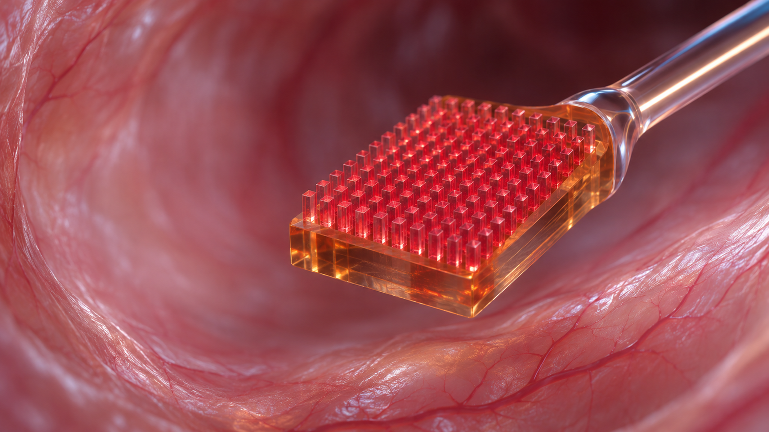
Physicists at the University of Science and Technology of China in Hefei have built arrays of silicon carbide quantum sensors whose detected photon count rates run ten to twenty times higher than typical values for the same sensors in a flat crystal. They used the devices to pick up nanoscale nuclear magnetic resonance signals from hydrogen nuclei a few nanometers above the chip, at room temperature.
The work appeared as a preprint on 12 November 2026. The hardware sits several steps away from any clinical instrument. Sensors made from atomic defects in crystals can feel the magnetic fields of single molecules, but they are faint, and they are hard to make by the thousand with the same performance. The Hefei group reports progress on both counts, using a material the semiconductor industry already processes on full wafers and sensors that are both excited and read out with near-infrared light, which the authors expect to cause less light damage in biological samples than the green light that pumps most diamond sensors.
What the Laboratory of Spin Magnetic Resonance in Hefei reported on 12 November 2026
The paper, "Bright and Uniform Silicon Carbide Nanophotonic Arrays for Scalable Nanoscale Quantum Sensing" on arXiv, comes from Chenyang Liao, Chihang Luo, Xin Chen, Cunliang Xin, Hongfang Zuo, Haoyu Sun, Fazhan Shi, Mengqi Wang and Ya Wang. Mengqi Wang and Ya Wang are the corresponding authors. The group works at the Laboratory of Spin Magnetic Resonance in USTC's School of Physical Sciences and at the Hefei National Laboratory. The manuscript has not yet been through peer review.
The sensors are two kinds of light-emitting defects in the 4H form of silicon carbide, known as PL5 and PL6 centers. Each defect carries an electron spin whose response to a magnetic field can be read out with a laser and a microwave signal, a technique called optically detected magnetic resonance. In earlier work these centers gave stable signals at room temperature, with a typical detected count rate of about 100,000 photons per second in bulk crystal. The weak signal is a direct limit on sensitivity, since the measurement improves with the square root of the light collected.
The team shaped the crystal surface into tiny pillars, each 480 nanometers tall with a top radius of 310 nanometers, so that more of the defect's light leaves the crystal and reaches the microscope. Simulations predicted that this geometry collects about 54 percent of the light from a PL6 center and 32 percent from a PL5 center with an air objective of numerical aperture 0.7. They also showed that the gain disappears quickly when the defect sits off-center in the pillar.
Quantum pillar: sensing. Technology readiness: TRL 3 of 9. In Quentir's assessment, the sensor chips work on real hardware in a physics laboratory and detected hydrogen nuclei in a drop of microscope immersion oil; no cell, tissue, blood or patient sample has been measured with them yet.
How self-aligned fabrication and oxygen ion implantation put the defects in the right place
Placing an atomic defect at the center of a pillar is the hard part. The group used a self-aligned two-layer photoresist process in which a single electron-beam pattern defines both the spot where oxygen ions enter the crystal and the metal mask that later shapes the pillar around that spot. The two steps are aligned by construction, which keeps the implanted region within a radius of about 45 nanometers of the pillar's axis. The PL5 and PL6 centers then form during high-temperature annealing after implantation at 15 and 3 kiloelectronvolts.
The measured brightness matched the simulations. Two representative centers reached detected saturation count rates of 1.25 million photons per second for PL5 and 2.20 million for PL6. Across 19 PL5 and 17 PL6 centers chosen at random, the average was 1.03 million photons per second for PL5, with a standard deviation of 0.07 million, and 1.92 million for PL6, with a standard deviation of 0.24 million. The authors describe these detected count rates as a new benchmark for silicon carbide color centers; the gain comes from collecting more of the light, since the defects themselves are unchanged. The pillars added negligible background light, and the magnetic resonance contrast of the defects stayed at the level reported in bulk crystal.
Why near-infrared light and wafer-scale silicon carbide could help biological and medical sensing
Nitrogen-vacancy centers in diamond are the established quantum sensors in biology. Researchers at Harvard used them in 2013 for optical magnetic imaging of living magnetotactic bacteria, published in Nature, and in 2016 a Harvard team reported nuclear magnetic resonance detection and spectroscopy of single proteins in Science. Diamond nanopillars of the kind the Hefei group now makes in silicon carbide already serve as probes for biological magnetic resonance and scanning magnetic imaging, as the authors note.
Silicon carbide offers two practical differences. Its PL5 and PL6 centers are pumped and emit in the near-infrared, which the authors say reduces light damage to living samples, avoids much of the background glow that tissue produces under visible light, and couples well into optical fibers. The material is also compatible with CMOS chip manufacturing and is already produced on large wafers, while single-crystal diamond is not. For a future diagnostic device, that combination points to chips that could carry many identical sensors and be made in a conventional foundry. Quentir's coverage of Fraunhofer IAF's diamond sensor inside a laser cavity, aimed at measuring brain signals outside shielded rooms, showed the diamond route working on a different problem: the sensitivity of larger magnetometers.
What the proton NMR test in immersion oil shows, and what it leaves open for clinical use
To test the devices as sensors, the team placed microscope immersion oil on the chip and used a PL5 center about 6.5 nanometers below the surface to detect the magnetic resonance of hydrogen nuclei in the oil. The measurement ran at 645.58 gauss with a dynamical decoupling pulse sequence. Repeating it at several field strengths gave the gyromagnetic ratio of the proton, which confirms that the signal came from hydrogen nuclei. The authors report a two- to threefold gain in magnetic field sensitivity over earlier NMR work with PL5 and PL6 centers, which they describe as comparable to leading nanoscale sensing with diamond.
For a clinician or a hospital buyer, the gap to practice is clear from the paper itself. The test sample was oil, a standard calibration material with a dense and uniform population of hydrogen nuclei. The paper reports no measurement on proteins, cells or tissue, no study of how the sensors behave in water or blood, and no packaging into a probe or an instrument. The authors frame the arrays as building blocks for scanning probes based on atomic force microscopy and for sensor networks in research settings.
What diagnostics and hospital research teams can look for in the next papers from Hefei
Three results would show whether silicon carbide can follow diamond into biological measurement. The first is a measurement on a biological sample, such as a protein layer or a living cell, with the sensitivity reported in the same units as this paper. The second is a comparison of light damage and background signal between near-infrared silicon carbide and green-pumped diamond on the same sample. The third is a wafer-level yield figure: how many pillars on a full chip contain a working, correctly placed defect. None of the three requires a clinical trial.
Sources
Primary source: preprint by Chenyang Liao, Chihang Luo, Xin Chen, Cunliang Xin, Hongfang Zuo, Haoyu Sun, Fazhan Shi, Mengqi Wang and Ya Wang (University of Science and Technology of China and Hefei National Laboratory), arXiv, 12 November 2026. Also drawn on: diamond quantum-sensing studies by Le Sage and colleagues (Nature, 2013) and Lovchinsky and colleagues (Science, 2016), and earlier Quentir coverage.